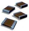
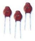
Surface mount:
SMD component sizes are usually defined in terms of their approximate size in hundredths of an inch. For example, a ceramic SMD capacitor (or resistor) which is .126 inch long by .063 wide is called a "1206" size. SMD tantalums however, are usually defined by their size in tenths of a millimeter. So, a 1206 tantalum is called a 3216 (3.2 mm long by 1.6 mm wide). Tantalums also have letter codes. A 3216 is commonly called an "A" size. Some versions have an "L" version for low profile. An A tantalum (3216) is 1.6 mm high while the AL is 1.2 mm high. All L versions have a maximum height of 1.2 mm, while non-L tantalums can go as high as 2.9 mm. The "L" versions have their own letter designation. Manufacturers don´t always follow the standard letter designations, especially with the low profile versions. There is a chart of who uses what at: http://www.kemet.com
For ceramics, usage is steadily shifting toward the smaller sizes. 603 is now the most popular size world wide, with 1206 in decline. The same thing is happening to SMD tantalums as the largest sizes are starting to disappear.
Not all capacitor materials are suited for surface mounting. Types available include ceramic, porcelain, polyester, PEN, PPS, mica, paper-epoxy, thin-film, and both electrolytics. Second-sourcing can be a problem with SMD film capacitors. Few vendors make them as present, and those that do differ significantly in their manufacturing capabilities.
Ceramic capacitors are the life's blood of the SMD capacitor market. Selection is more limited than for through-hole capacitors. Most manufacturers tend to stick to the big three, C0G, X7R, and Z5U, with some adding temperature compensating capacitors. A few also make X7S and Y5V; some others can be found if you look hard enough. Ceramics come in several package styles. Leadless chip capacitors are by far the most common, but large ceramics (>1 uF) come in a number of "J" and "L" lead-frame variations, some made up of more than one chip.
As the use of SMD parts has increased, there has been plenty of competition among capacitor types, driven largely by the need for better, low-ESR capacitors for high-frequency power applications like switching power supplies. Aluminum capacitors have been improved to compete with tantalums (although tantalums have steadily improved), ceramic capacitors have grown larger to compete with aluminums and film capacitors have grown larger to compete with large ceramics. Makers of large (to at least 20 uF) SMD metallized-film polyester capacitors, like ITW Paktron, have been pushing them as substitutes for Class 2 ceramic capacitors in some applications. The advantages offered include negligible aging, no loss of capacitance from applied voltage, and fewer problems with soldering. Also, unlike ceramics, metallized film capacitors can self-heal and are unlikely to fail short (if there is enough energy to clear the short).
However, SMD capacitors have also grown steadily smaller for use in portable equipment like pagers and cell phones. Tantalums have benefited from improved tantalum powders and better packaging for a steadily increasing capacitance-to-size ratio and have become available in smaller sizes. Both ceramic and tantalum makers pursue innovative designs to get low ESR and inductance for power supply bypassing in high-speed digital systems.
For RF and microwave applications, a variety of SMD parts are used. C0G ceramics are the most common, but mica, porcelain, and thin-film types (see AVX-Kyocera ACCU series) are also used.
Wound:
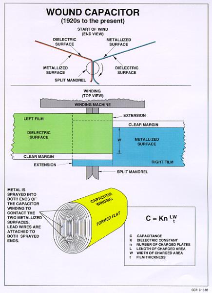
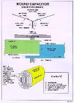
The first plastic film capacitors were constructed by attaching leads to the narrow ends of two long, rectangular pieces of aluminum foil and winding them together with an insulator in between. Not a great idea since this forms a serious parasitic inductor. A better way is to wind the foils so that all of one edge for each foil is exposed, then short all the edges together and attach the leads. OK, it's hard to visualize the way I describe it. This allows the current to flow in a shorter and more-or-less straight line. Almost all film capacitors are now made this way or in stacked-foil form. Most aluminum electrolytics are still made the old-fashioned way, but some have multiple connections to each foil.
Some wound-film capacitors have a band at one end to show which lead is attached to the foil on the outside. That lead would be the one to go to ground or some other low-impedance point in certain applications to either prevent noise pickup, or reduce radiated noise.
Metallized film vs. film/foil:
An alternative to using aluminum foil is to metallize the two sides of the dielectric by vapor deposition. This makes for a smaller capacitor, results in self-healing capability, and is the most common construction now used. If a spot on the dielectric breaks down, the arc will usually clear the aluminum film from around the hole by vaporizing it (this assumes that enough energy is available to clear the short). Some film capacitors are "precleared" during manufacturing to blow away pin-holes and weak spots in the dielectric. Metallized film capacitors tend to have a higher ESR than film-foil, however, and somewhat lower insulation resistance. Film-foil capacitors are typically 50-150 % larger in volume than their metallized-film equivalent. Some types, especially for high-voltage and pulse applications, have more complicated constructions. For example, a polyester carrier film metallized on both sides and separated by a polypropylene film (the dielectric layer) or floating metallized layers to form a metal-PP-metal-PP-metal sandwich. Other variations include foil layers separated by metallized layers to get reduced ESR yet still allow for self-healing, and even foil and metallizing in the same electrode layer. In most cases, the idea behind these various constructions is to get the good self-healing of a metallized-film capacitor with the low ESR/high current capacity of film/foil.
Although aluminum is the most common metal used as the metallization or foil material, other metals are sometimes used (if only rarely) including copper, zinc, silver, tin, and tin-lead. Aluminum is hard to beat for cost and reliability. Proprietary alloys are now used in large, high-voltage film capacitors for more reliable self-healing. Zinc has been used for its better healing properties, but it is more vulnerable to corrosion. Self-healing is absolutely critical for long-term reliability for high-energy film capacitors. One method to improve self-healing is to "segment" the metallization. Instead of metallizing all of the film, the metallization is laid down in many square or diamond-shaped patches which are connected by narrow metallized "bridges". If one segment suffers a catastrophic failure the segment is isolated from the others by the bridges which act as fusible links. However, self-healing by this mechanism can result in a progressive loss of capacitance, a potential problem in some applications.
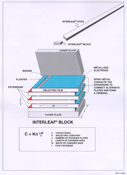
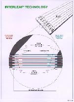
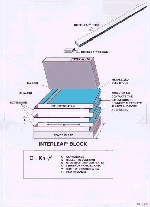
Stacked film and film/foil:
Another way is to stack the foils and insulator in alternating flat layers instead of winding them. This makes for a compact form-factor and low inductance. Both foil and metallized types are made this way. Pictures below copyright ITW Paktron.
Multi-lead:
If two leads are good, more leads are better. At least in high-frequency/high-current applications. Large (>1 F) film capacitors and ceramic capacitors are available with 4+ leads (both through-hole and SMD lead-frame) to reduce lead induction and ESR. Some vendors stack several ceramic SMD capacitors and add multiple leads to make one very large ceramic capacitor with a minimum footprint. I have seen at least five chips stacked vertically and at least 20 horizontally. This allows for very large (and/or very high voltage) ceramics, such as C0G >10 uF and Z5U >1000 uF. Some equipment manufacturers solder several SMD capacitors together on edge to achieve the same thing. Some capacitor makers even list separate ESL numbers for vertical and horizontal soldering.
Nonmagnetic:
SMD ceramic capacitors with nonmagnetic end terminations for use in very high magnetic fields (in the several Tesla range).
Most capacitors have silver-palladium outer electrodes covered by a nickel barrier layer, and solder or tin over the nickel. The
nickel is to prevent leaching of the silver during soldering. Nonmagnetic types have silver-palladium outer electrodes with a
copper barrier. Commonly used in nuclear magnetic imaging machines (NMI or NMR). Non-magnetic capacitors were once
relatively rare, but today almost anyone who makes SMD ceramics or trimmer capacitors makes then in non-magnetic versions.
Non-magnetic film capacitors have been seen (at least as specials) as have SMD tantalums.
Capacitors available in non-magnetic versions:
Ceramic, C0G and X7R, both SMD and with leads.
Films.
Trimmers, in ceramic, polymers, Teflon and sapphire. You can also get non-magnetic mounting hardware.
Acrylic SMD.
Tantalum SMD.
Teflon non-SMD (Polyflon).
Also...Resisters, connectors and coils (air core).
Feedthru:
Feedthru ceramic capacitors are used for high frequency filtering. This configuration minimizes the affect of parasitic induction.
Some are designed for feeding through a panel or a terminal block. Some are made for filtering an entire multiline connector.
4-terminal:
Some SMD electrolytics are available in a 4-terminal configuration for reduced lead inductance. This technique can raise the
resonance frequency from its typical 100-500 kHz to well over 1 MHz. It is especially useful for polymer-based aluminum
electrolytics where it reduces the already low high-frequency impedance.
Fused:
Some tantalums for power supply bypass are available with integral fuses. Not a bad idea. As mentioned elsewhere,
backwards tantalums can take a long time to fail, and when they do, fire and smoke may be involved. It will increase the ESR
however.
The large polypropylene motor run and start capacitors usually contain a fuse of a sort. A pressure or temperature sensitive
disk causes a wire to break if the capacitor overheats.
Spark-Gap Capacitors:
These ceramic capacitors have a slot sawed in them to form an integral spark-gap to protect "sensitive" components from voltage transients and static buildup. The capacitors were typically of up to 0.02 uF of Y5P or Z5U material, and the gap is typically rated from 1 to 6 kV, with a tolerance of 300-500 VDC. They may also be sold with the gap only, no capacitor. A very few manufacturers still make these.
Voltage ratings:
The various electrolytics each have their own upper limits of working voltage, beyond which no parts are available. These are mentioned elsewhere. The common plastic films seem to have no particular limit on working voltages however, polypropylene capacitors at least, are available with working voltages in the 100s of kV.
Actually, obtaining parts with the minimum possible working voltage is more important to many users. At one time, the typical capacitor had an operating voltage in the range of 100s to 1000s of volts. Such capacitors are still readily available, but in numbers sold, they are the exception. As equipment has gotten smaller (pagers, cell phones), the demand has been for ever higher volumetric efficiency. The way to get it is with thinner dielectric layers, if you reduce the dielectric thickness by half, the capacitance-per-volume increases by a factor of four (this assumes the electrodes take up negligible volume). For system voltages of 5 volts and below, the ideal dielectric thickness is in the micron region, a few microns for ceramics and less than one micron for film dielectrics. This would give an operating voltage no higher than the system needs, and highest capacitance in the space available. This is a problem for capacitor manufacturers who have not yet found it possible to reliably produce such thin dielectrics. They are getting close however.
The breakdown voltage of dielectrics drops as temperature increases. Many manufacturers list a rated operating voltage that applies over only a part of the capacitor's temperature range, most often to 75 or 85C. Above that, a derating of 1.1-1.5 %/C must be applied. Read the data sheet carefully.
Frequency also affects working voltage. Manufacturers will usually give a DC voltage and an AC voltage, with the AC voltage specified to be 60 Hz (50 for the Europeans). Pulse-rated capacitors (sometimes others as well) will generally have an AC working voltage specified for some higher frequency, plus, there may be a graphical guide for derating at higher frequencies. Other manufacturers will just have a dV/dT rating.
Oddly enough, the breakdown voltage for dielectric films is usually nonlinear. For thicknesses greater than about 5 mils, the breakdown voltage increases very roughly with the square of the film´s thickness (4 times the thickness gives 2 times the breakdown voltage, sort of). Below 5 mils, the breakdown voltage tends to be dominated by defects in the film, which makes it more linear but relatively lower. Tables in different handbooks and manufacturer's literature use a variety of thicknesses to list breakdown voltage (volts/mil for a 1/8", at 1", or at 1 mil thicknesses for example). Worse yet, measured breakdown voltage depends on other factors such as how long the voltage is applied, the shape of the electrodes, and the quality of the dielectric (freedom from physical defects and chemical impurities). All this makes it difficult to compare dielectrics unless everything you want to know can be found in the same table, and you have some assurance that all the dielectrics were tested the same way. Manufacturers often say their tests, (voltage breakdown, dissipation factor, etc.) are done to ASTM standards. See ASTM D-149 and D-150.

Capacitor Construction and Special Features.
Packaging:
A variety of packaging methods are used for film. The main concern is moisture penetration. Moisture will diffuse through most
plastics fairly quickly. Epoxy is much better than most polymers, and is commonly used as the sealing material in better
capacitors . Only metal and glass are (almost) 100% resistant to gas and liquid diffusion.
•The naked film chip. Used for both leaded and SMD parts, this style has always worried me. Variations include a
layer of tape over the chip, and epoxy over the ends to help hold the leads. Not, I would think, recommended for
humid environments.
•A step up is the popular "wrap and fill" package. A layer of tape goes over the capacitor, and the ends are sealed with
epoxy. This is probably good enough for moderately humid environments.
•Another step up is the boxed capacitor. The wound capacitor is put in a molded box and potted in epoxy. This is
good for high reliability in humid environments. Most XY line-filter caps use this construction. A variation is heavy
epoxy encapsulation without the box.
•The ultimate in reliability is the hermetically sealed capacitor. Used for military, and critical industrial applications, the
container is metal, and the leads are sealed with glass.
Electrolytic:
Aluminums are almost always in an aluminum can with a rubber end seal. Better aluminums have an epoxy seal over the rubber,
mostly to keep out cleaning solvents. Most aluminum package innovations are directed toward better cooling for high ripple-
current applications. A few large aluminums have an integral bolt for chassis mounting for better heat sinking. A few others
come in flat packages to increased surface area for better convection cooling. Most SMD aluminums are in a small (but
otherwise conventional) can in an unsealed plastic box, or have just a plastic base to hold the leads. True molded packages
may soon appear. True hermetic sealing is unlikely for conventional aluminum electrolytics with liquid electrolytes. They evolve
trace amounts of gasses that must be vented. Aluminums using conductive polymer electrolytes are found in molded packages
and are a better candidates for hermetic packages.
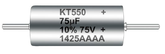
Thru-hole tantalums are usually epoxy dipped, some have molded packages, or are hermetically sealed. SMD tantalums are
molded in epoxy.
Ceramic:
Ceramics are mostly sealed in epoxy. A few are glass encapsulated.
Mica:
Mica is more vulnerable to moisture than most capacitors. Older mica capacitors were molded, a rather violent process. The
newer dipped micas are somewhat more reliable. Some have hermetic packages.
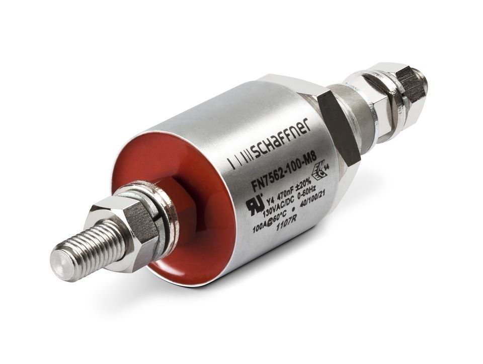
Hermetic Packaging:
Hermetic capacitors have been around for a long time. They were more common in the days of small paper-in-oil capacitors that were more vulnerable to humidity than most modern capacitors. Wet tantalums, dry tantalums, film capacitors and ceramic capacitors all benefit from being separated from the environment, but they are not cheap. For some newer polymer electrolytes which are exceptionally sensitive to humidity and oxygen (like PEDOT), they are almost mandatory, at least at high temperature. Hermetic sealing of classic aluminum capacitors is unlikely. Aluminums evolve trace amounts of gas that needs to be slowly vented off.
Hermetic capacitor are now rare in many dielectrics, but they are common for tantalum and paper and there are now hermetic aluminums. There are also some ceramic capacitors and ceramic trimmers that are called hermetic. If you really need hermetic film parts, a number of specialty companies make them as specials.
What is a hermetic seal? The definition is hard to pin down. The dictionaries say it is a seal that will block all air and moisture. Not very realistic in real life however, it's hard to detect that last molecule of water to prove or disprove "all". I assumed that to be hermetic you could only use glass, ceramic and metal in the seal because polymers have notoriously high diffusion rates for gasses and vapors. By and large this true. But even with metals, hydrogen, helium, and other gases have some small diffusion rate, and glass absorbs gasses from the atmosphere. Epoxy is probably the best sealing material and even that is forbidden under MIL-STD-883, the "Bible" of microelectronics testing for hermeticity. However, molded PEEK and Viton O-rings are sometimes mentioned in connection with some "hermetic" connectors. Also, plastic pouches for sealing food are sometimes referred to as hermetic, a total misuse of the word. "Hermetic" may be what you say it is, depending on your requirements, but MIL-STD-883 is where many people start.
Hermetic parts are mostly used in military, aerospace, and industrial applications where humidity or corrosive gasses are a problem. The prices are high enough to limit their use.
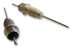
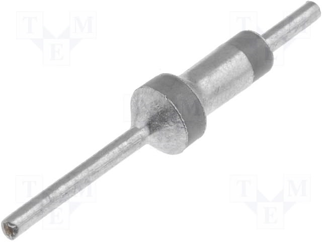
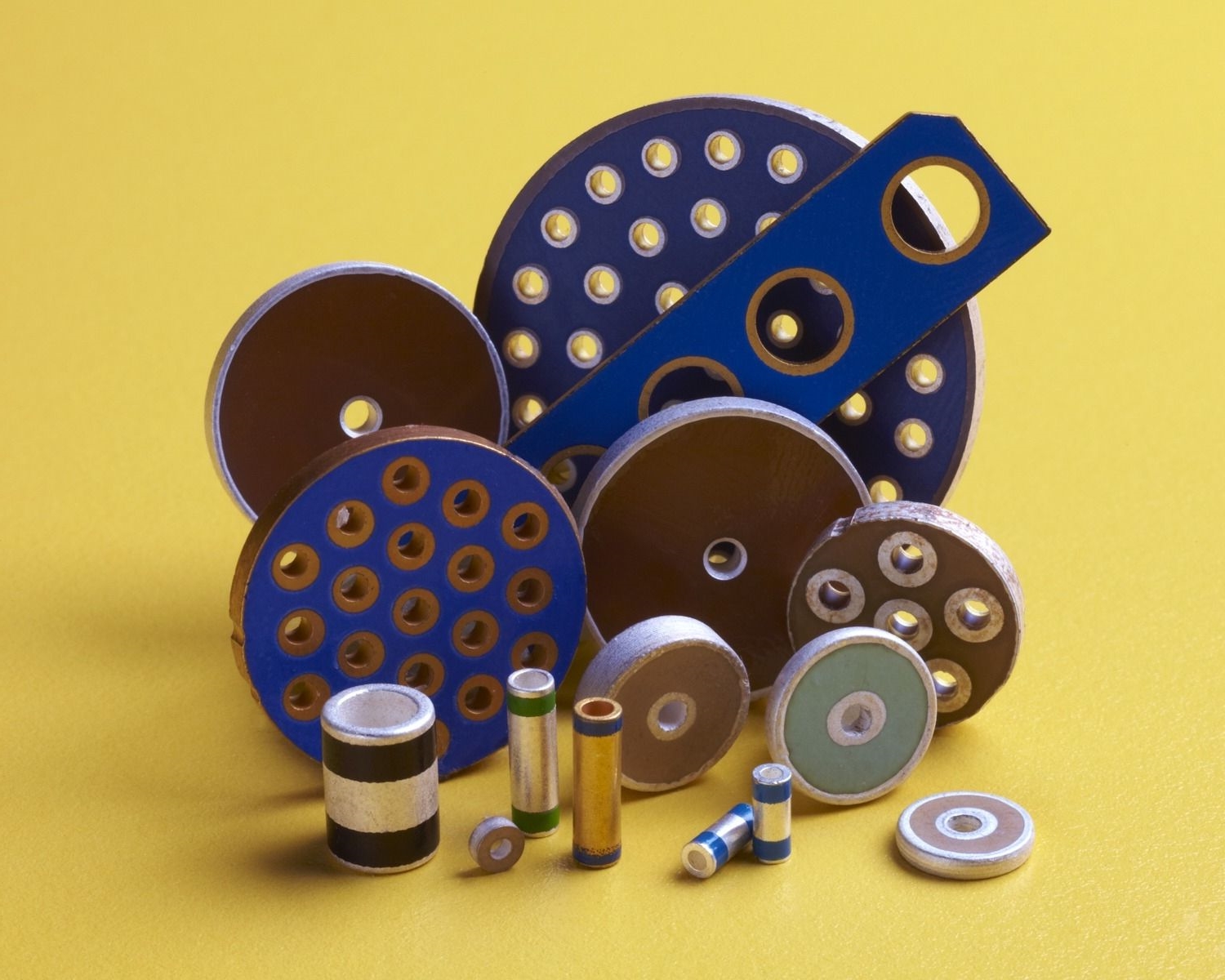
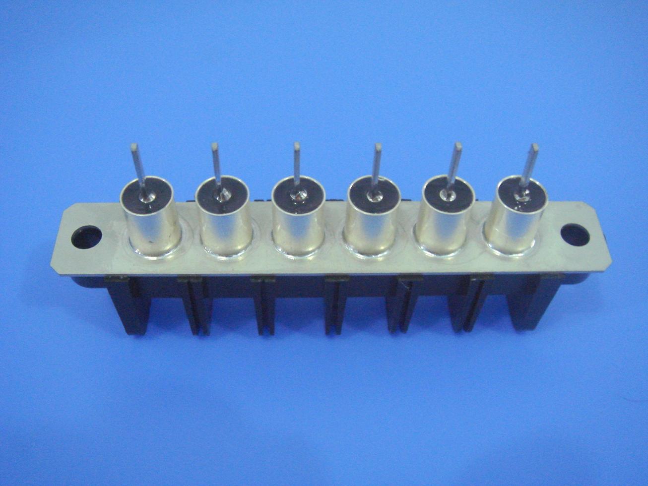
To the right are pictures of a few of the many hermetic packages. And a package that is not as hermetic as the manufacturer claims. Hermetic capacitors are made much the same as other hermetic parts, usually in metal+glass. Metal packages can only be used for lower voltage parts, <1000 volts, because additional insulation would be required. Ceramic and glass can be used for higher voltage parts because the package is its own insulation.
Double click to edit